DS18B20
17 of 22
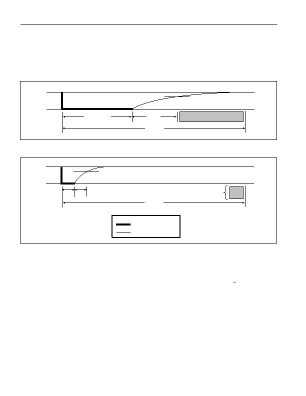
data from the DS18B20 is valid for 15祍 after the falling edge that initiated the read time slot. Therefore,
the master must release the bus and then sample the bus state within 15祍 from the start of the slot.
Figure 15 illustrates that the sum of T
INIT
, T
RC
, and T
SAMPLE
must be less than 15?/SPAN>s for a read time slot.
Figure 16 shows that system timing margin is maximized by keeping T
INIT
and T
RC
as short as possible
and by locating the master sample time during read time slots towards the end of the 15祍 period.
Figure 15. Detailed Master Read 1 Timing
Figure 16. Recommended Master Read 1 Timing
RELATED APPLICATION NOTES
The following application notes can be applied to the DS18B20 and are available on our website at
www.maxim-ic.com
.
Application Note 27: Understanding and Using Cyclic Redundancy Checks with Maxim i
Button Products
Application Note 122: Using Dallas' 1-Wire ICs in 1-Cell Li-Ion Battery Packs with Low-Side N-Channel
Safety FETs Master
Application Note 126: 1-Wire Communication Through Software
Application Note 162: Interfacing the DS18x20/DS1822 1-Wire Temperature Sensor in a Microcontroller
Environment
Application Note 208: Curve Fitting the Error of a Bandgap-Based Digital Temperature Sensor
Application Note 2420: 1-Wire Communication with a Microchip PICmicro Microcontroller
Application Note 3754: Single-Wire Serial Bus Carries Isolated Power and Data
Sample 1-Wire subroutines that can be used in conjunction with Application Note 74: Reading and
Writing i
Buttons via Serial Interfaces can be downloaded from the Maxim website.
V
PU
GND
1-WIRE BUS
15?/SPAN>s
VIH of Master
T
RC
T
INT
> 1?/SPAN>s
Master samples
LINE TYPE LEGEND
Bus master pulling low
Resistor pullup
V
PU
GND
1-WIRE BUS
15?/SPAN>s
VIH of Master
T
RC
=
T
INT
=
small
Master samples
发布紧急采购,3分钟左右您将得到回复。
相关PDF资料
DS2740U+T&R
IC CURRENT GAUGE(15BIT) 8UMAX
DS28EA00U+T&R
IC THERMOMETER 1-WIRE 8-USOP
DS3920T-001+
IC CURRENT MIRROR 5:1 SOT23-6
DS4560LS-LO+T
IC SWITCH HOT-PLUG 12V 8-SOIC
DS600U+T&R
IC SENSOR TEMP 8-USOP
DS620U+
IC THERMOMETER/STAT DIG 8MSOP
DS7505U+T&R
IC DGTL THERMOMETER 2WIRE 8-USOP
DS75LVU+T&R
IC SENSOR TEMP DIGITAL 8MSOP
相关代理商/技术参数
DS18B20Z+
功能描述:板上安装温度传感器 Prgmble Resolution 1-Wire Parasite Pwr RoHS:否 制造商:Omron Electronics 输出类型:Digital 配置: 准确性:+/- 1.5 C, +/- 3 C 温度阈值: 数字输出 - 总线接口:2-Wire, I2C, SMBus 电源电压-最大:5.5 V 电源电压-最小:4.5 V 最大工作温度:+ 50 C 最小工作温度:0 C 关闭: 安装风格: 封装 / 箱体: 设备功能:Temperature and Humidity Sensor
DS18B20Z+
制造商:Maxim Integrated Products 功能描述:SEMICONDUCTOR ((NW))
DS18B20Z+T&R
制造商:Maxim Integrated Products 功能描述:HI RES MICROLAN DIG THERM 8-SOIC TR 制造商:Maxim Integrated Products 功能描述:TEMP SENSOR DGTL SERL (1-WIRE) 8SOIC N - Tape and Reel 制造商:Maxim Integrated Products 功能描述:IC THERM MICROLAN PROG-RES 8SOIC 制造商:Maxim Integrated Products 功能描述:Board Mount Temperature Sensors Prgmble Resolution 1-Wire Parasite Pwr
DS18B20Z+T&R
功能描述:板上安装温度传感器 Prgmble Resolution 1-Wire Parasite Pwr RoHS:否 制造商:Omron Electronics 输出类型:Digital 配置: 准确性:+/- 1.5 C, +/- 3 C 温度阈值: 数字输出 - 总线接口:2-Wire, I2C, SMBus 电源电压-最大:5.5 V 电源电压-最小:4.5 V 最大工作温度:+ 50 C 最小工作温度:0 C 关闭: 安装风格: 封装 / 箱体: 设备功能:Temperature and Humidity Sensor
DS18B20Z-W
制造商:Maxim Integrated Products 功能描述:
DS18S20
功能描述:板上安装温度传感器 RoHS:否 制造商:Omron Electronics 输出类型:Digital 配置: 准确性:+/- 1.5 C, +/- 3 C 温度阈值: 数字输出 - 总线接口:2-Wire, I2C, SMBus 电源电压-最大:5.5 V 电源电压-最小:4.5 V 最大工作温度:+ 50 C 最小工作温度:0 C 关闭: 安装风格: 封装 / 箱体: 设备功能:Temperature and Humidity Sensor
DS18S20/T&R
制造商:Rochester Electronics LLC 功能描述: 制造商:Maxim Integrated Products 功能描述:IC THERM MICROLAN HI PREC TO-92
DS18S20/T&R
功能描述:板上安装温度传感器 RoHS:否 制造商:Omron Electronics 输出类型:Digital 配置: 准确性:+/- 1.5 C, +/- 3 C 温度阈值: 数字输出 - 总线接口:2-Wire, I2C, SMBus 电源电压-最大:5.5 V 电源电压-最小:4.5 V 最大工作温度:+ 50 C 最小工作温度:0 C 关闭: 安装风格: 封装 / 箱体: 设备功能:Temperature and Humidity Sensor
